11. 💻 Introduction to Computer Hardware and Architecture
This chapter provides a brief introduction to how a computer functions internally — from physical components to machine-level instruction execution. It is based on material of geeksforgeeks, inf-schule and AI.

Video for Kids
11.1 🧩 Major Hardware Components
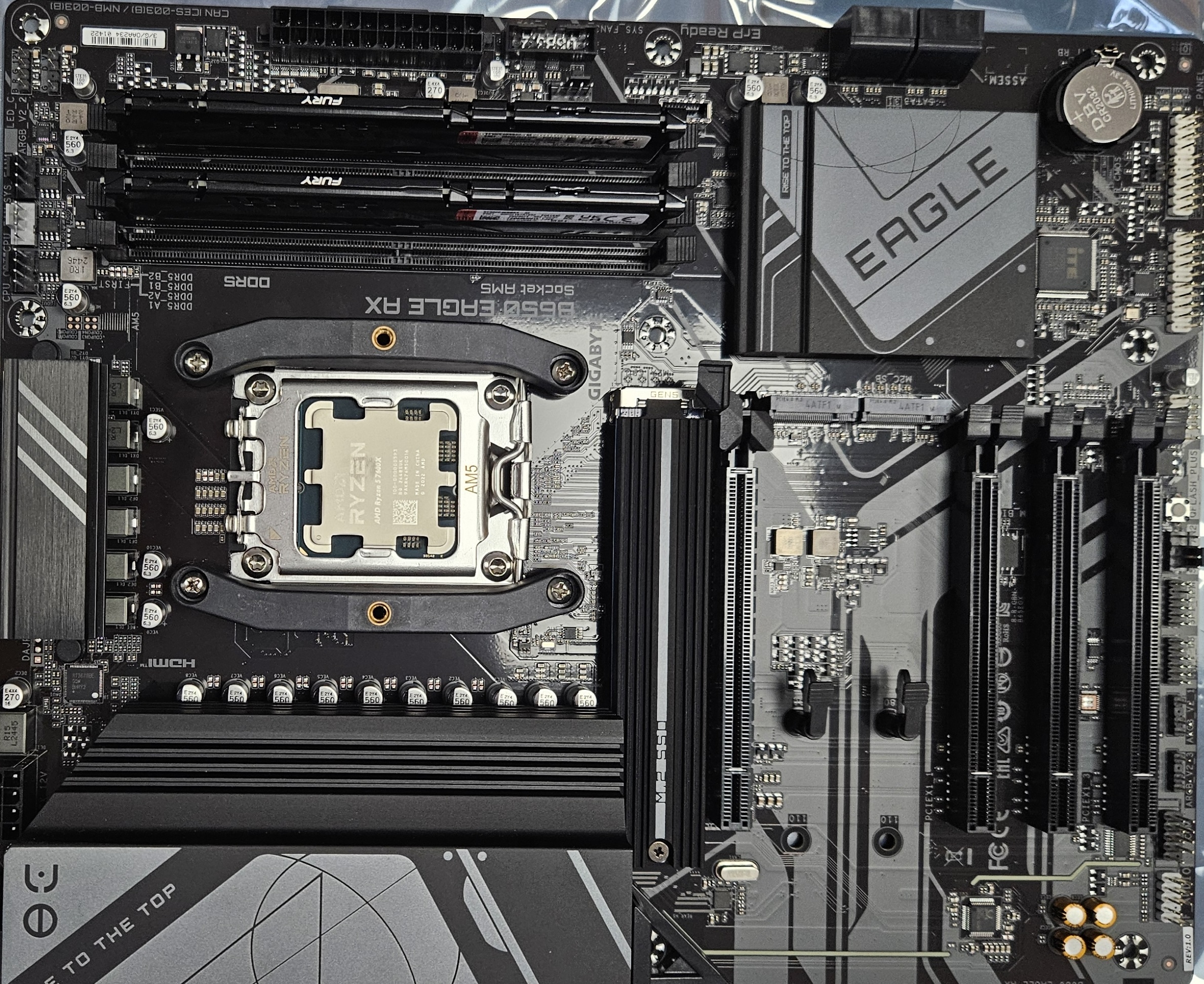
The motherboard is the main circuit board that connects all components together. It houses the CPU socket, memory slots, expansion slots (PCIe), and various connectors for storage and peripherals. Think of it as the nervous system of your computer, providing pathways for data and power distribution.
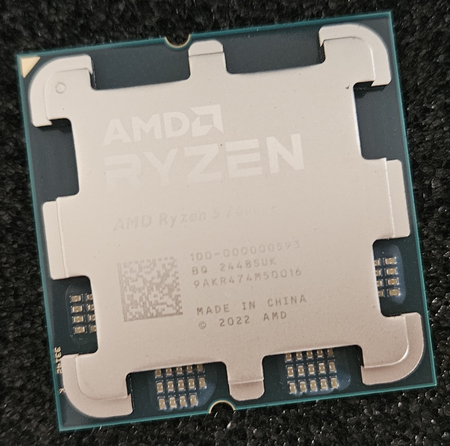
The Central Processing Unit (CPU) is the brain of the computer, executing instructions and performing calculations. Modern CPUs contain billions of transistors organized into functional units.

Transistors are the fundamental building blocks of modern electronics. These tiny semiconductor devices, typically just a few nanometers in size, have three connections - two as input and output electrodes.
Key performance metrics include
- Clock speed (GHz): The number of cycles the processor executes per second. A higher clock speed typically means faster execution, but efficiency also depends on architecture.
- Cores: Modern CPUs have multiple cores, each capable of executing instructions independently. A quad-core CPU can handle four tasks in parallel.
11.1.1 Memory Hierarchy
- RAM (Random Access Memory): Fast, volatile memory where the operating system, active programs, and current data reside.
- ROM (Read-Only Memory): Non-volatile memory containing essential firmware (e.g. BIOS) needed to boot the system.
- Cache: Small and ultra-fast memory located inside or very close to the CPU. Cache stores frequently accessed data to speed up processing.
11.1.2 Graphics Card (GPU)
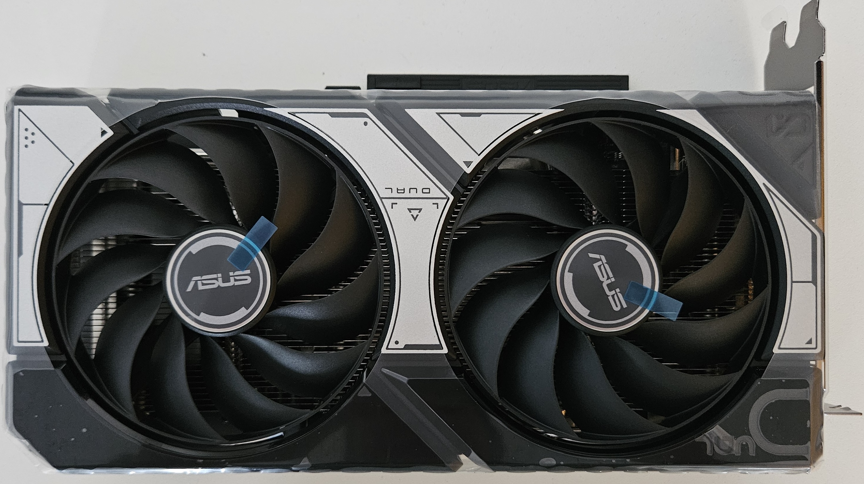

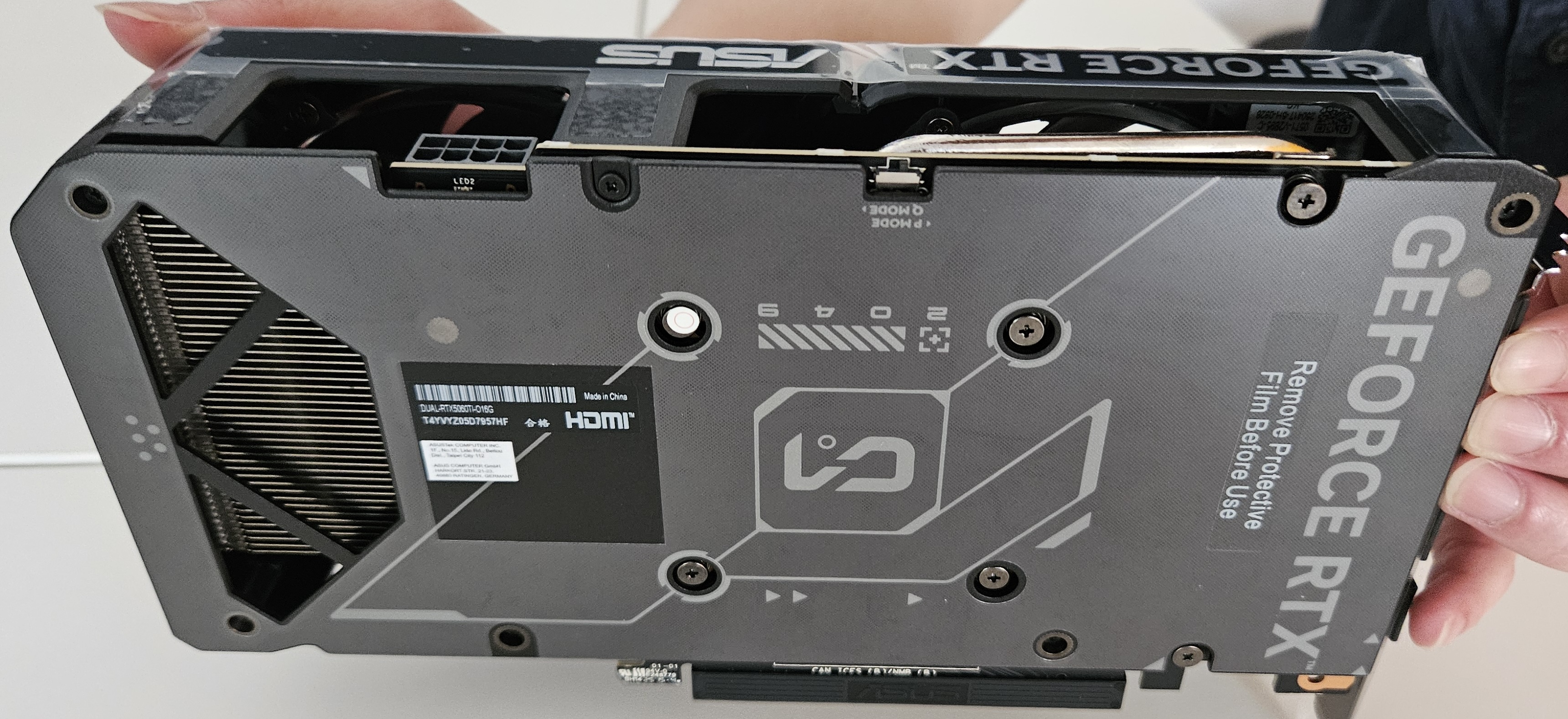
A Graphics Processing Unit handles rendering of images, video, and animations. Modern GPUs are highly parallel processors and are widely used in gaming, scientific computation, and AI/machine learning tasks.
Unlike CPUs, which have a few powerful cores optimized for sequential tasks, GPUs consist of thousands of smaller cores that can process many operations in parallel. This makes them ideal for tasks where the same operation needs to be performed on large amounts of data simultaneously.
In the context of AI, training a model often involves performing billions of matrix operations. GPUs can accelerate this process dramatically by distributing these calculations across their many cores.
Parallelization means splitting a task into many smaller subtasks that can run at the same time. GPU offloading refers to shifting those subtasks from the CPU to the GPU, which can process them more efficiently in parallel.
However, achieving good parallel performance depends not just on the hardware but also on the software. Well-designed algorithms are required to effectively divide the problem into subtasks that:
- Can be run independently,
- Minimize communication overhead,
- And make efficient use of GPU memory and processing pipelines.
For example, training a neural network with millions of parameters using only a CPU might take days or weeks. Running the same task on a modern GPU can reduce training time to hours or even minutes. This is why GPUs (and increasingly TPUs – Tensor Processing Units) are critical in AI research and production systems.
11.2 ⚙️ Logic Circuits and Binary Operations
At the lowest level, all computation in a computer happens through binary logic — manipulation of 0s and 1s via logic gates.
11.2.1 Boolean Logic Gates
| Gate | Function | Symbol | Truth Table Example |
|---|---|---|---|
| NOT | Inverts input | ¬A | A=1 → ¬A=0 |
| AND | A and B | A∧B | A=1 B=1 → 1, else 0 |
| OR | A or B | A∨B | A=0 B=0 → 0, else 1 |
| NAND | NOT of AND | ¬(A∧B) | A=1 B=1 → 0, else 1 |
11.2.2 NAND Game (Digital Logic Design)
The NAND game is an educational tool that shows how all other logic gates (AND, OR, NOT) can be constructed using only NAND gates. Since NAND is functionally complete, it demonstrates the principle that any digital circuit — even an entire CPU — can be built using a single type of logic gate.

11.2.3 Half-Adder
A half-adder is a basic digital circuit that adds two single binary digits (A and B). It has two outputs:
Sum (S): A ⊕ B (XOR) — represents the result bit
Carry (C): A ∧ B (AND) — represents the overflow or carry to the next bit
Half-adders are the foundation for full adders, which additionally handle input from previous carries. Together, they form the basis of multi-bit binary adders in processors.
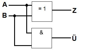
These simple logic blocks eventually scale into full arithmetic logic units (ALUs).
11.3 🧠 The CPU and Control Unit
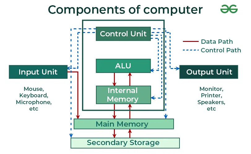


A typical CPU contains
- Arithmetic Logic Unit (ALU): Performs arithmetic and logical operations.
- Control Unit (CU): Directs operations and manages the CPU's workflow.
- Registers: Small, fast storage within the CPU for temporary data
11.3.1 Registers
Registers are small, fast memory units inside the CPU. They hold data, instructions, and addresses during processing.
Types of registers:
- General-purpose: Temporarily hold data and results
- Instruction Register (IR): Holds the current instruction
- Accumulator (ACC): Used in older/simple CPUs to store results
- Status Register (FLAGS): Contains condition flags (zero, overflow, negative)
- Program Counter (PC): The Program Counter is a register that stores the address of the next instruction to be fetched. After fetching, it typically increments to point to the next instruction, unless a jump or branch modifies it.
- Stack Pointer (SP): Tracks the top of the call stack (used in function calls and recursion)
11.3.2 ALU (Arithmetic Logic Unit)
The ALU is the part of the CPU responsible for performing arithmetic operations (add, subtract, multiply, divide) and logic operations (AND, OR, NOT, comparisons). It works in tandem with registers and receives control signals from the control unit.
11.3.3 Control Unit
The Control Unit orchestrates the actions of the CPU. It:
- Fetches instructions from memory
- Decodes them into signals
- Activates relevant parts of the CPU (ALU, registers, memory access)
It acts like a traffic manager, making sure instructions are executed in the correct order.
11.3.4 🔁 CPU Instruction Cycle (Fetch-Decode-Execute)
The core of CPU operation is a repeated sequence known as the instruction cycle:
- Fetch: The next instruction is retrieved from memory.
- Decode: The control unit interprets the instruction.
- Execute: The instruction is carried out — using ALU, registers, or memory.
- Store: If the instruction modifies data, the result is written back to memory or a register.
graph TD
  Start --> Fetch --> Decode --> Execute --> Store --> Fetch
11.4 Architecture
11.4.1 Von Neumann Architecture
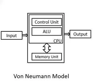
Proposed by John von Neumann, this architecture uses a single memory and bus system for both program instructions and data.
Issue: If the CPU needs to fetch data and an instruction at the same time, it must wait — causing the Von Neumann bottleneck.
11.4.2 Harvard Architecture
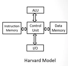
This design uses separate memory and buses for instructions and data, allowing simultaneous access and faster performance. It is commonly used in microcontrollers and signal processing hardware.
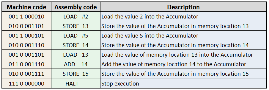
11.5 🧾 Machine Code
Machine code is the binary language understood by the CPU. Each instruction is a fixed-length sequence of bits, typically 32 or 64 bits long.
Each instruction is represented by a binary pattern that includes:
- Operation code (opcode)
- Target register
- Source register
- Immediate or memory address (if needed)
11.6 Simulations
There are many simulators to better understand, how computers work.
- Bonsai-Modellrechner
- JOHNNY-Modellrechner
- inf-schule
- zum material
Assemblercode